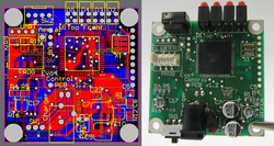
Warped PCBs

You just got a nice big PCB back from the fab shop. You set one on your desk to admire only to discover that it’s warped. What do you do?

There are two primary types of causes of board warping: process related at the fab or assembly shop, and layout-related issues. If it’s warped before assembly, it’s between fab and layout. If it’s flat before assembly and warped, after, it’s most likely between layout and assembly — although sometimes a fab problem won’t show up until a pass through the reflow oven at your assembly partner.

Determining the root cause is generally a bit of an iterative process. It’s tempting to start right off with your fab or assembly partner, but you need some information before giving them a call. You’ll need such things as the amount of warpage per inch, board size and thickness. With that, you need to take a good look at your design and consider copper pours, component size and component placement.

With that information in hand you can make your phone call. If the board is warped before assembly, call your fab shop. If it’s flat pre-assembly and warped post-assembly, call your assembly house.

The shop you call will want to talk over your design to help you pinpoint the cause. If you can rule out a design issue,then you need to talk with your partner to determine whether it’s a fab or assembly issue and next steps to take care of you.

 Here are a few design issues that could contribute to warping:

  • Uneven copper pour. Copper and FR-4 are a good match relative to thermal expansion, but they aren’t exact. A large pour on one side or corner of your board can lead to warping due to dissimilar expansion characteristics. This could cause warpage either at the fab shop or the assembly house.
  • Components with large thermal mass grouped together on the board. This would be more likely to cause problems during assembly than during fab. The thermal mass will act as a heat sink for that area on the board, which can lead to uneven expansion and uneven soldering.
  • A board that’s too thin for the size or number of components could lead to warping at any stage.
  • Odd shapes or large cutouts could also lead to warping at any point.

There may be other, more obscure causes, but those are the main design related causes. If it’s none of those talk with your partner.

Occasionally, design requirements lead to a board that is essentially non-manufacturable. Hopefully you never have this situation, but if you do, make sure that thickness, component location, pours, or cut outs really, really, really, need to be the way they are.

If you absolutely, positively can’t change anything, go back and try again. Then you can to look for heroic means to get the board fabbed and built.

Slight warpage might go away when the board is mounted. Just be careful with that. Some components may not stay securely soldered when you flatten it.

The board may need a special fixture during assembly to prevent warping. This will likely cost extra, but if you can’t change your design, and still need it built, it may be your best option.

Finally, if nothing works, you may need to look harder at the design, or look for a new fab or assembly house. We all like to think we can do just about anything, but every shop has its limits, and on rare occasion those limits can be difficult to spot.

Duane Benson
What if Godot was late because he was waiting for John Galt?

http://blog.screamingcircuits.com

Component Packages — Let’s Get Small

I’ve been on a bit of a package binge lately. First talking about metric vs. US passive sizes, and then a very tiny ARM Cortex M0 from Freescale.

The Freescale BGA part checks in at 1.6 x 2mm. That’s cool and I’m almost always in favor of making things as small as possible, but, as I wrote in my prior blog on the subject, it’s not always possible. The 0.4mm pitch BGA is problematic unless you can spend a lot of money on the raw PCBs, or will have super high volume.

All is not lost, though. You still can use a tiny ARM Cortex M0 part. Just not quite as tiny. That same part also comes in a 3 x 3mm QFN package. You lose four pins (16 vs. 20) going from the BGA to the QFN, but if you can handle that, it’s a very viable option that doesn’t require any exotic circuit board technologies.

A few years ago QFNs were scary, but not so much any more. I’ve designed a few of them in using Eagle CAD. Just be sure to pay attention to the footprint. A 6 mil trace is more than small enough for a 0.5mm pitch QFN.

Duane Benson
Strive at all times to bend, fold, spindle and mutilate

http://blog.screamingcircuits.com/

Collins Closing

Count me among those sorry to hear the news that Rockwell is closing its printed circuit board fabrication plant.

I’ve been through that plant and this is sad to see. I wrote a profile of the plant for PC FAB in 2000. At the time, then GM Mike Driscoll was overseeing a major implementation of Lean manufacturing, making the site one of the early adopters of the practice.

I’m of the opinion (minority, probably) that OEMs retaining in-house knowledge and expertise of manufacturing processes is a good thing, even if they can’t necessarily generate a direct profit from it.

That, plus I knew several people who worked in that shop over the years and every one of them is a class act.

There are still a few major OEMs with in-house fab capacity. Let’s hope they see fit to keep it.


Updating the Design Standard

IPC-2221A, as most designers know, was released in 2003. Since that time, lead-free has gone from a niche technology to a mainstream one, and its added a generous dose of complexity to the design decision tree.

In November, IPC-2221B was, at long last, released, and it’s a good opportunity to reflect on the process of how standards are developed, and why it took nearly a decade to get the latest rev out.

In that time, for example, the task group responsible for J-STD-001, the industry soldering standard, came out with a “D” and an “E” revision, and work is underway on the “F” revision.  Certainly the changes lead-free brought about affected electronics assembly at least as much as design: it’s hard to pin the problem solely on technical reasons.

My experience working on the J-STD-001 suggests the difference in publishing frequency comes down to how the respective task groups call a halt to the changing technology. Going back to when Jerry Rosser was chair of the J-STD-001, for example, that group has a 15-year-plus history of calling a hard stop to new technical additions after a set period of time. Jerry knew the standards would always be disrupted by new technology, and therefore he initiated a plan — still followed — whereby after a period of months, the spec would be frozen, and the only changes from that point to the revision in progress would be to ameliorate the grammar and, on the rare occasion, fix legitimate technical disputes. If, for example, new chip-scale package requirements weren’t ready by the hard stop, they were tabled for the next rev. The ensuing document was never perfect, but it was far more timely than would have been otherwise possible.  To wit, the task group published four revisions, plus one amendment, in one decade alone.

Based on interviews with the coordinator of the IPC-2221, a different tack was taken, which slowed the process considerably.  It took the task group several years before calling a hard stop. Another difference is the decision to include a fair amount of tutorial in the design standard, whereas the soldering task group stripped all that info out years ago, opting instead to segment it into a separate handbook.

Now, to be sure, there is a design guide, but it was published in 1992 and has never been updated. I understand the philosophical reasons for doing things the way the design task group has done them, but in the interest of faster time-to-market, I think it’s time to reconsider whether there’s a better way. Thoroughness has value. But so does expediency.

Associations in Agreement

Taiwan’s Vice President Wu (tallest man, center of photo) welcomed visitors and took part in the ribbon-cutting ceremony for the TPCA Show held in conjunction with the IMPACT 2012 event in Taipei. Second from the right is IPC CEO and president John Mitchell.

The TPCA and the JPCA signed a Memorandum of Understanding at the Taipei Nangang Exhibition Center on Oct. 25 to highlight industrial cooperation in a practical and efficient way. The TPCA organized an Alliance Seminar held in conjunction with the endorsement. This followed the Advance Technology Forum alliance event of this past July. The activity is supported by Taiwan’s Economic Department. Approval of funding was announced after the signing.

IMPACT 2012 was jointly organized by IEEE CPMT-Taipei, iMAPS-Taiwan, ITRI and the TPCA, and co-organized by IDB-Ministry of Economic Affairs, I-Shou University, NanKang IC Design Incubation Center. SMTA, and TTMA. IMPACT (International Microsystems, Packagiing, Assembly and Circuits Technology Conference) attracted 190 papers from 14 countries.

The TPCA held a special breakfast presentation in which an update on the industry in Japan (PCB domestic production down 45+% from its peak in 2007 as offshore manufacturing increased) by Dr. Hayao Nakahara of NTI and the industry status in Thailand presented by Bancha Ongkosit, chairman and managing director of KCE Electronics. The latter stated that Thailand lacks supply chain infrastructure and that he no longer buys from the US. He pointed out the growth of automotive electronics, stating that virtually every major car company as set up there, and that Thailand exports about 3.5 million vehicles per year. He also stated that the growth of organic substrate replacement for ceramic based electronic circuits for vehicles will continue to increase rapidly.

America’s Interdyne Systems, a new fabrication equipment entry debuted its revolutionary new concept for the mechanical drilling of 75 micron holes. Taiwan Kong King (TKK) celebrated its 35th Anniversary at the show.

It’s a Collaborative World After All
Rumors persist that an announcement of a new collaborative activity between the IPC and iNEMI is imminent.

Lenovo, the world’s second largest PC producer, will start production of its Think brand notebooks in the US next year at its fulfillment center in North Carolina. Lenovo acquired IBM’s PC division (original producer of the Think PC) in 2005. Last month Lenovo announced the acquisition of Brazil’s PC maker Comercio de Component Electronicos.

Taiwan’s intelligence chief warned that one in every three Taiwanese companies based on the mainland are facing closure due to rapidly falling profits, according to Agence France-Presse in Taipei. Another 30% are also reported to be struggling on the mainland. Last year the island’s authorities approved 575 mainland investments totaling $13.1 billion.

Removal of Conformal Coating with Small Sandblasters

Development of conformal coating technology was driven to a large degree by the military and aerospace industries. While conformal coatings are mostly used on populated, printed wiring boards (PWBs), they are also used to protect components such as transistors, diodes, rectifiers, resistors, integrated circuits (ICs) and hybrid circuits including multichip modules (MCMs) and chip-on-board (COB).

Recent environmental regulations and concerns have had a significant impact on both coating materials and application methods, particularly with regard to control of volatile organic compounds and chlorofluorocarbon compounds. VOCs and CFCs have been extensively used as solvent carriers. Manufacturers and suppliers of conformal coating materials have responded by developing non-solvent based coatings and environmentally acceptable methods of application, curing and removal.

It is important to consider how the choice of a conformal coating material affects the rework and repair issues. The need for rework or repair of a conformal coating can occur any time after completion of an assembly due to a variety of process or product requirements and component replacement issues.

A number of methods are available for rework of conformal coatings. These include thermal, chemical, mechanical, plasma and laser-based systems and small sandblasters or “micro abrasive blasters,” which will be the focus of this column.

Micro-abrasive blasters used for conformal coating removal are small sandblasting systems that are commonly used for metal deburring and etching as well as surface preparation. The cutting media is introduced into a compressed air stream and is ejected through a hand piece utilizing tips as small as 0.026″. This is directed at a component or surface area on PCB where the conformal coating has to be removed. This system can remove conformal coating from a single test node, an axial leaded component, a through-hole IC, an SMT component or an entire PCB without any modification to the system for a variety of coating materials. This method provides the most practical and environmentally friendly means for removing conformal coating from PCB assemblies.

Although these small Micro Abrasive Blasters provide the most practical and environmentally friendly means of removal, they also pose a problem. Micro Abrasive Blasters can generate static electricity as the high velocity air and particles impinge on the PWB surface. The ESD voltage generated at the point of contact can cause damage to components and electrical circuits on an assembly.

Equipment manufacturers have used several different approaches to solving the ESD problem. These are: 1) the installation of AC or DC pulsed ionizer bars in the chamber results in a rapid decay of ESD voltages in the work cell and tubing 2) the installation of a point ionizer at the end of the nozzle to dissipate any static charge built-up in the media stream at the point of contact 3) the use of an inline, auto balanced ionizer where the air source is split, one side flowing to the media and the other side flowing to the inline ionizer. This ionized air is then injected into the media stream just before it leaves the nozzle, eliminating the static charge buildup in the media chamber. The ionized air is also pumped into the work chamber. With this type of system, ESD levels are reportedly in the +10V range.

Whose Fault Is It, Anyway?

The change in administration at IPC will inevitably dredge up lots of the past as various factions position themselves for a seat at the table.

Those whom hew to the line that IPC’s emphasis over the past decade has shifted to the assembly market are correct: IPC followed the money, and since the massive shift of printed circuit board fabrication to Asia starting in late 2001, assembly has where the North American money has been.

But that assessment  just as inevitably turns to anger and blame — fingers get quickly pointed at IPC for somehow failing the domestic PCB market. I’m not sure that’s justified.

IPC’s interest in programs for fabricators has waned; of that, there is no doubt. But it has waned in large part because fabricators themselves stopped supporting those programs. The PWB Presidents Meetings and the TMRC are shells of their former selves, it says here, because the members stopped forcing the issue. Keep in mind, IPC has long followed a “build it and they will come” model. That’s not a good strategy for a trade association. But fabricators who abdicated leadership over the IPC share much of the responsibility for what it’s become. It’s not that the IPC board of directors no longer reflects the needs of small guys so much as it’s that the board no longer reflects the needs of the private owner, large or small. No one complained IPC wasn’t doing enough for fabricators when representatives from large fabs like Photocircuits were on the board.

Could IPC provide better direction for the North American fabrication industry? Yes. But the Chinese have done just fine without the help of a strong domestic association. Given that, it’s hard to argue that IPC was the cause of the decline. Back in 2000, when the forecasts for high layer count boards were staggeringly optimistic for the foreseeable future, old friend Jack Fisher lamented that it would keep the domestic industry from investing in HDI for another couple years. He was right: none did. Then the bottom fell out, and none of them had the cash to invest in the newer technology, thus relegating them to third tier status. As one who participated in the IPC Technology Roadmap going back to its first incarnation, I can say microvias were clearly expected to take hold. In that respect, the IPC did its part; the industry just didn’t follow.

It’s uncomfortable to admit we got beat, and no, the playing field with China has never been level, and yes, IPC’s lobbying and related activities have been confused and ineffective, but there’s plenty of blame to go around, and not all of it was a trade group’s fault. We’d all be better off, I think, to focus on the needs of the future rather than the sins of the past.

Another Tidal Wave Hits Japan

Old friend Dominque Numakura comes back from the annual JPCA Show with a stunning announcement: Japan’s PCB industry seems to be on life support.

From a series of dull presentations to the outsourcing of manufacturing to a general lack of optimism, the mood is dour, Numakura says. More ominous, some veterans are comparing the trend to the decimation of the US PCB industry in late 2001.

As late as 2000, the US and Japan were neck-and-neck in annual PCB sales, with the US dominating the large board space and Japan leading in HDI. Despite the problems experienced in the US, Japan continued to be the technology leader in PCBs, leading some to surmise that its vast investment and wise decisions on which technologies to focus on made Japan impervious to the cost pressures that sunk the North American industry. Numakura’s essay suggest that’s not the case, leaving one to wonder what this means for the circuit board industry for the coming decade.

How Not to Trick Your BGA Friends

Continuing with yesterday’s theme, I have a couple examples that should have been fine, but due to issues at the board house, improper storage or contamination, ended up very much not fine.

What is wrongBehind door number one, we have an OSP finish that will make you very unhappy. That’s “Organic Solderability Preservatives” in long hand. I’ve also heard it called “Organic Surface Preservative”, but close enough. It is a nice flay surface which is good for BGAs. Years ago, it had a reputation for being poor quality, “cheap”, but newer formulas seem to work pretty good in both leaded and lead free. In this case, the darker pads were likely contaminated in some way – either at the board fab house or subsequently in handling.

Siver migration problemNext is the worst example of surface degradation I’ve ever seen. Yes, it’s an extreme outlier case, but this is where a silver board can go if it wasn’t built with the best quality control, was stored too long, was exposed to polluted air or other contamination and had bad luck. This board probably has all of those issues, but any one alone can be problematic. Silver board especially should be stored in a cool dark place; preferably sealed in the original packaging.

Duane Benson
OSP can also mean Oregon State Patrol, but they don’t care about BGAs. Just safe driving.

http://blog.screamingcircuits.com/

Future Shock in Modern Times

By the time we round the corner into 2013, I will enter my 20thyear in the PCB and electronics industry. I find myself often gravitating to others like me (50 years and older) to swap nostalgic war stories of days gone by.  My journey in the industry, unlike my cronies, is marked by a 12-year hiatus that began around 1998 when I made the decision to stay home and raise my two young daughters full time. I resurfaced in 2010, with nearly grown kids, totally clueless about the state of an industry that I had all but forgotten.
Rip Van Winkle
For this reason, I possess a rather unique perspective, not unlike that of Rip Van Winkle waking from a prolonged slumber.  Some things have changed dramatically, while other things seem unaltered. The greatest “future shock” that I experienced upon reentry was the fact that people had all but ceased to speak to each other or meet face to face (apart from coworkers) preferring rather the more efficient use of emails and texts. The sophistication of voice mail systems had evolved so radically that they secured decision makers into cozy office-bunkers. Phones rang far less, and real-live receptionists had nearly gone extinct! I quickly adapted to the brave new world and became a speed-typing, computer-dependent, Linked In guru. I am now fully integrated into the modern day business sensibilities of 2012. Phew!

Last week Transline was exhibiting at the Del Mar Electronics and Design show, and I was asked to do a one-hour talk. I decided my topic would be How to Fall in Love with Your PCB supplier. I meant it to be a tongue-in-cheek comparison to John Gray’s relational model of Mars and Venus, and how suppliers and customer relationships contain a similar tension. I sought to identify the areas of disparity and offer ways to reconcile these differences—noting that much of these are a result of poor communication and not talking to each other!  For research, I went on Linked In and asked people what they loved and hated about working with PCB suppliers. I received some excellent feedback and blended that with my near 20 years of experience, having worn my share of hats and gaining multiple perspectives—including my Rip Van Winkle viewpoint.
I would like to share some of the input I received along with the input of the dozen or so folks that showed up for my talk. I hope you will find it as fascinating as I did! I will also chime in with my own opinions for what attributes add up to a really effective “lovable” PCB supplier. I will also attach a paper I wrote with the culmination my findings. Until next time … Live long and prosper!

— Judy